Editor’s note— This is a rather high-level article explaining the major setbacks in the launch of our SM200A 20 GHz spectrum analyzer. In addition to being transparent about the delay, we hope to offer some valuable technical information for those planning or troubleshooting their own electronics manufacturing processes.
We’ve got some ‘splainin’ to do
Okay, okay. We’re a little behind schedule with our new 20 GHz spectrum analyzer, and it’s probably time to explain a few things.
I believe we once stated that our new SM200A spectrum analyzer would be available for retail in July of 2017. This was probably around the end of 2016. And if we didn’t state it, we certainly (at least internally) thought we would have it for sale by then.
As time pressed on, though, things started to slip a little. That July target turned to August, and then August turned to September.
We thought September 2017 was a lock. After all, it had been nearly three years since development officially started on our new 20 GHz Spectrum Analyzer, and with the progress made during the summer months, we were pretty sure we were good to go.
Perfection seemed so close. With just a little more time… we could… have… it… even more… perfect. We took the loose shipping deadlines as an opportunity to tweak the hardware and software in an effort to make first version of the SM200A even better.
However, some early discussions with potential clients started locking us into shipping timelines, and people were seriously starting to look for a defined delivery date for the spectrum analyzer. The proverbial “cat” was inching its way out of the bag.
By the time we hit the IMS tradeshow in Honolulu in June of 2017, we were sure October would be the time we could start shipping SM’s. So sure, in fact, that we started publishing the October date in print and on our website.

Whoops. And double-whoops, considering the editor’s note.
It was at this point that things were all coming together. In the summer of 2017 all signs were pointing to a definite October launch. The integration of SM200A-specific code into Spike’s codebase was going smoothly. The early beta versions of the analyzer were working reasonably well. All in all, the device and timeline were looking solid.
But believing we were close to done was our mistake. Up until now things were more-or-less in our hands and under our control. It was when we started ordering the final production quantities of parts that the notion of shipping the device on time became suspect.
Entering the world of unknowns
Now, this isn’t our first rodeo, and we’ve been manufacturing hardware for years. But this was the first time we’ve put together a device this complex and we had to figure a few things out.
Issues with the RF board
Our first major hiccup, occurring during the transition from engineering to the production line, was with the RF circuit boards being used in the analyzer. Like many in the electronics industry, we have our bare circuit boards produced by a third-party (sometimes referred to as a board house). When working with the board house we specify the exact circuit board design (known as a stackup) which consists of multiple layers of copper and laminated substrates. We also specify the thickness and the type of copper and substrates to be used in the stackup. Yet another third-party vendor (known as a contract manufacturer) then handles populating the bare boards with the electronic parts we provide. This process involves the placement and soldering of thousands of tiny components to the bare circuit boards.
One of the stages in building the bare board assembly is called etching, which is where unwanted copper is removed from a printed circuit board to create traces. These traces act like tiny wires connecting all the components on the board. During the design process we specify the thickness of the copper layers on the board in units of ounces of copper per square foot.
We designed our RF board stackup with four total layers of copper, with one-ounce of copper on layers one and two, and a half-ounce copper on layers three and four. Thinner copper on layer four meant that the board house could order industry-standard, in-stock material as opposed to ordering cores with different copper weights on each side. Our goal was to reduce material ordering lead-time with this design.
In reality, though, the use of the unbalanced copper layers (along with our use of epoxy fills under certain components) resulted in undercutting during the etching process1, which caused the thinnest traces and/or filter elements to delaminate, as shown in the picture, making the board unusable.
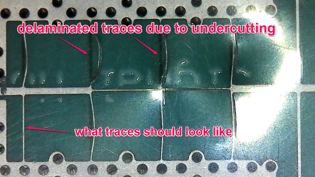
The nasty effects of undercutting on our boards (as viewed under a microscope)
After a string of miscommunications (nobody’s fault in particular – just good ol’ fashioned communication issues) over the period of a few weeks and way too much wasted money in scrapped RF boards, it was finally determined that a custom order of laminate cores with one-ounce copper on one side and half-ounce copper on the other side should fix the problem. It simply meant that layer four of the stackup had to be one-ounce copper instead of half-ounce copper. Our RF engineer approved this new design, the new material was ordered, and boards were successfully built.
With the RF board issues sorted out and shipped to our production facility, we were finally able to proceed with testing. Although well past our advertised product launch date, we were at this point hoping for good news. And some of the news was good – the new stackup created boards that were more resilient, resulting in fewer failures and much more consistent performance.
But something was still off. Dang it.
Wandering RF energy
Our testing process puts our devices through a variety of demanding activities across extremely hot and cold conditions, making sure our analyzers are accurate and stable across temperature fluctuations to simulate real-world use. During our testing we observed excessive spurious responses measuring way beyond our expectations – not in a good way. After inspection, it was apparent that the contact surfaces between the device housing’s interior cavity walls and the circuit boards weren’t tight enough to keep the RF energy created within each cavity from leaking into adjacent cavities. The result was an unacceptable level of spurious signals2.
With the targeted spurious performance of the SM200A out the window, we knew something had to change – either that, or we had to relax our spec sheet to reflect this undesirable performance. We wanted to avoid compromising spurious performance, if at all possible.
Researching the subject revealed that applying a pliable conductive electromagnetic interference (EMI) gasket to where the cavity walls contacted the circuit boards should provide adequate internal shielding, helping to keep RF energy within the device in its intended space. This would be easy enough. Just distribute the gasket along the edge of chamber walls within the device and we’re done – or so we thought.
It turns out that EMI caulking is a bit finicky and didn’t want to stick to our e-nickel (electroless nickel) plated housing. We experimented with a few housing modifications to get the caulking to stick better, and even bead blasted the inside of the housing to slightly “rough up” the finish in order to get the EMI material to stick. The bead blasting unfortunately had the opposite effect and ended up decreasing the available surface area to which the caulking could stick3.
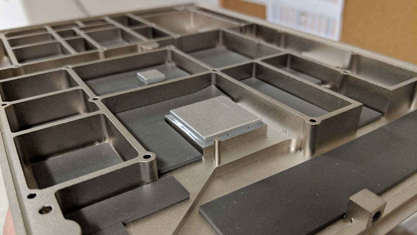
The culprit, in all its un-gasketed glory.
Hmm… Who knew? (Actually there’s probably someone that knows and we really wish we could locate them, but alas…) What we did know, at this point, is that we had a genuine head-scratcher on our hands.
This troubleshooting process also taught us that EMI caulking sticks adequately to most e-nickel chemistries, but it does not stick well to all e-nickel chemistries. The EMI caulking provider we are working with told us that they have problems with EMI caulking adhesion to e-nickel with less than 10% of their jobs. Unfortunately for us, we seemed to have landed in this small percentage.
Then, finally – after weeks of research, opinion-seeking and several failed attempts – we learned about a certain cleaner and primer combination that would make the EMI caulking adequately adhere to our housings. This combination of prep chemicals was applied to a handful of our housings, the EMI gaskets were applied, and the housings were sent our way (we received them just last week, in fact). We are happy to report that the EMI gasket is solidly in-place, firmly attached to the SM’s housing and it’s ready to isolate the RF energy within the device.
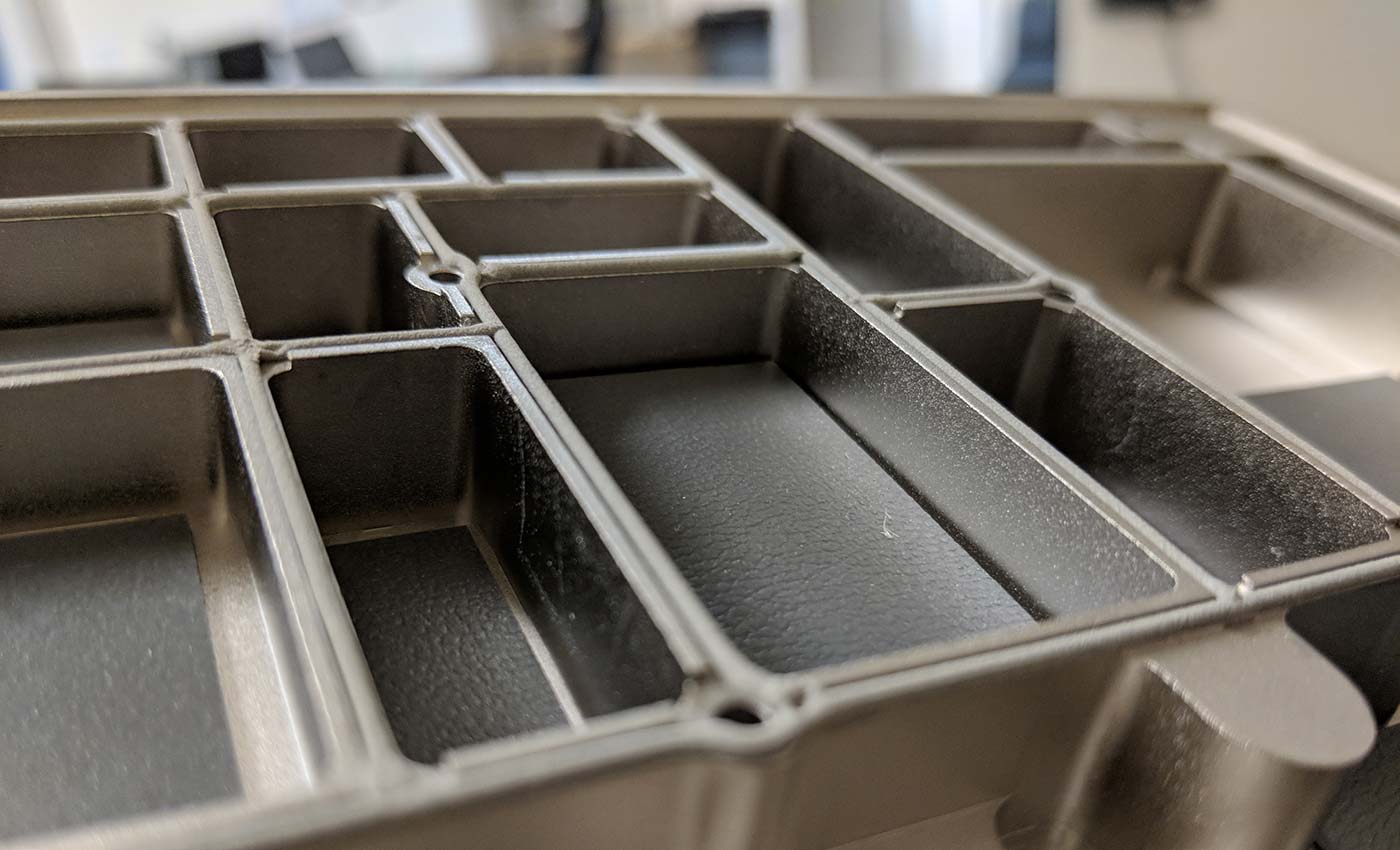
EMI caulking in-place, ready to work.
Back on track (and just a wee bit behind)
As of today, February 6th, 2018, we have our first production SM200A spectrum analyzer built, tested, and nearly ready to send out the door to its proud new owner. Housings for future devices will be arriving from the machine shop in batches over the next couple of weeks, and production is ramping upward through the month of February (and yes – if you’ve been in contact with us regarding the status of your pre-ordered SM200A, you will be receiving your device shortly).
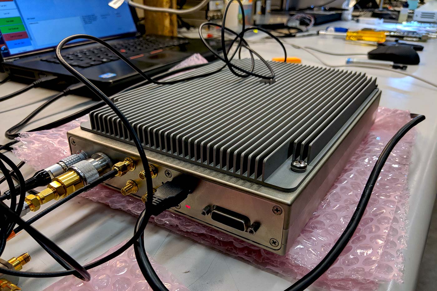
Coming soon, to a bench near you.
So, sure, we’re a bit behind. We wanted the SM200A shipping to customers last fall, but it just wasn’t in the cards. We can’t point fingers or place any blame, because everyone involved was working in unfamiliar territory, and anyone working in product development knows you can’t anticipate every setback. Additionally, the SM pushes some boundaries in terms of cost vs. performance and we had to navigate a lot of unknown territory to meet our goals.
What we do know, however, is that we work with some fantastic people and suppliers, and the knowledge gained from this process is invaluable.
We also know that the SM200A is one heck of a spectrum analyzer. Every time we went “back to the drawing board”, we ended up with a more desirable analyzer. The copper stackup we’re using on the RF boards results in less failures, increased device reliability, and minimized production issues. The cases for our devices are now tighter, providing a better-performing instrument with the low spurious performance we were striving for. So, in spite of all the delays, we’re glad we took the time to get it right.
Over the next few weeks, keep your eyes on the Products section of this site, as the SM200A will be appearing there shortly (and if this is the first you’ve heard about our new 20 GHz spectrum analyzer, you can learn more about it over here).
We certainly wanted to release our new instrument sooner, but trust that you’ll find it was worth the wait. We also believe that you are unlikely to find a better 20 GHz spectrum analyzer value for your money.
Footnotes:
1We also specified epoxy fills in some of the drilled and plated holes under certain components. This was needed to reduce soldering voids under these components. What we didn’t know, nor did the board house engineers know, is that we had created a toxically impossible combination of requirements for them to build.
There are small 5 mil (0.005”) wide filter elements, similar to traces on the top one-ounce copper layer one of the RF board. Combine this with half-ounce copper on the bottom layer four and it requires an unbalanced etch which creates a compromise in etch time between the thicker and thinner copper layers. Normally, this can be compensated for. But the epoxy fills put the board stackup over the edge.
When a board has epoxy fills added, the process then requires shaving a very small amount of the copper off the surface layers as the epoxy gets shaved smooth. This is normally not a problem but when you combine it with unbalanced copper weights on the outer layers then the 5 mil traces become difficult to not undercut during etching.
[return to article]
2To be totally honest, we were already aware of the presence of an unacceptable level of spurious signals in our early designs. Our intention was to greatly reduce the spurious signals by dividing the circuitry into several isolated sections using the machined housing cavities to create tight metal shields (essentially Faraday cages) around each circuit cavity.
We have been successful with Faraday shielding of our previous products by hand-soldering shields over sensitive circuits in the SA-series and the BB60C spectrum analyzers. But the SM200A has 28 sections which would require 28 hand-soldered shields if we were to take the hand soldered shield approach. This of course isn’t cost effective, which is why we utilized the Faraday cavity design.
[return to article]
3The EMI caulking is filled with tiny metal beads that make it electronically conductive. However, these beads prevent the caulking from flowing into the rough, bead-blasted surface – the caulking just sits on top of the rough surface.
[return to article]
15 Comments
Nice to see an open and honest account of what goes on behind the scenes, Thanks for the insight and best of luck for a successful launch of the SM200A.
Thanks Trevor. We appreciate that! We’re definitely seeing the “light at the end of the tunnel”.
Hello Cory . Bought the original Signal Hound / Tracking generator pair in May 2012. VF through VHF. Have watched you come a long way. Am a 16 years retired E.E with many years in design and development of communications hardware. Your story reflects the agonies of the day and as well as years past – same experience. While painful, it is always interesting and one learns important new things. constantly, even though the Boss is having fits. Keep up the good work… wish you continued success.
Thanks for the kind words John. You’re exactly right – the learning never stops. Just have to keep moving along, right? And thanks for the support, too. Our early customers are what got us this far!
Guys, you are doing a great job and we wish you a real success!
Thanks for the well-wishes Alexgor. We’re excited to finally get it into people’s hands.
We are looking forward to receive SM200 to include support of it by our RadioInspector.
Thanks for the honesty and hands up it was us line from Signal Hound! Too many times it’s a.n. others fault we went over on time! I’m truly looking forward to seeing what I’m hoping will be a great addition to the Signal Hound range! Once again thanks for the truthfulness in the update!! Regards, Stephen
It’s definitely been a learning experience! But what we’ve learned has been so important. Thanks for the comment Stephen!
This could be happened to everyone who build things from scratch, and this I believe you did all the way just to reach what we call “perfection”.. Great Success for SignalHound ????
Indeed Rishman, it’s always a challenge starting from ‘Ground Zero’. We appreciate the comments and support! Thanks.
Very interesting read, thanks. As a 40 year veteran of these RF battles I know this onion has many layers. One synthesizer I worked on had a solid milled plate with all the board compartments milled out. Along the top of the “fences” we had also milled channels where we placed RF gasket material. (O ring type) Screwing the lid over the plate brought these gaskets into slight compression. We were fighting spurs -140dBm or so. Keep up the good work.
Thanks Dino. There are many layers. Your product/challenge sounds relatively familiar to ours – it’s always nice to hear the realities of other peoples’s projects. Take care-
I used electroless Nickel on waveguides but then moved to tri-metal plating decades ago. You should explore it too, but you may have to use Zn die-cast for fencing, or some under plating on aluminium. I have now developed nickel allergy so get boils on palm as I touch nickel. But have been doing 140dB shielding so know what you talked about. Roughing the contact surface was a bad idea indeed. I will have more comments when I test SM200A first hand. Can’t wait!
Phenomenal article and candidness! Every electrical and mechanical engineer involved in product design and development should read and comprehend these events. More importantly, every person who wants to be a technical manager or product manager in a company that designs, develops and/or produces products for electronic communications needs to also study and learn from this example. Development of High Speed and/or RF/uW communications equipment is NOT EASY, nor does it follow typical ‘schedules’.
I have been watching the USB Test & Measurement product offerings over the last ten to fifteen years and I am extremely impressed by the products your company is producing to the market. Needless to say, it seems by your articles that you have just produced an extremely competitive Signal Analyzer instrument at a fractional cost of the big T&M vendors.